- 您现在的位置:买卖IC网 > Sheet目录343 > MIC3231YTSE (Micrel Inc)IC LED DRVR HP CONS CURR 16TSSOP
Micrel, Inc.
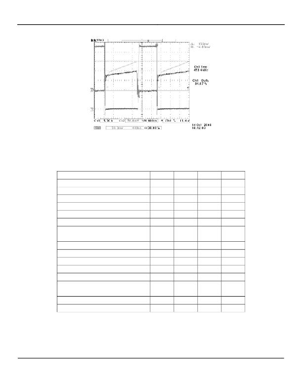
Figure 6. IS Pin and V RCS (Ch1 = Switch Node, Ch2 = IS Pin, Ref1 = V CS )
Design Procedure for a LED Driver
MIC3230/1/2
Symbol
Parameter
Min
Nom
Max
Units
Input
V IN
I IN
Input Voltage
Input current
8
12
14
2
V
A
Output
LEDs
Number of LEDs
5
6
7
V F
V OUT
I LED
I PP
PWMD
OVP
Forward voltage of LED
Output voltage
LED current
Required I Ripple
PWM Dimming
Output over voltage protection
3.2
16
0.33
0
3.5
21
0.35
40
30
4.0
28
0.37
100
V
V
A
mA
%
V
System
F SW
Switching frequency
500kHz
eff
V DIODE
Efficiency
Forward drop of schottky diode
80
0.6
%
V
Table 2. Design Example Parameters
March 2011
12
M9999-030311-D
发布紧急采购,3分钟左右您将得到回复。
相关PDF资料
MIC3263YML TR
IC LED DRIVER 6CH BKLT 24-MLF
MIC3287-24YD6 TR
IC LED DRIVR WHITE BCKLGT TSOT-6
MIC3289-16YD6 TR
IC LED DRIVR WHITE BCKLGT TSOT-6
MIC3291-18YML TR
IC PWM WLED DVR 1.8V 1.2MHZ 8MLF
MIC4100YM
IC DRIVER MOSFET 100V CMOS 8SOIC
MIC4102YM
IC DRIVER MOSFET 100V TTL 8SOIC
MIC4103YM
IC MOSFET DRIVER 100V CMOS 8SOIC
MIC4124YME
IC MOSFET DRVR DUAL NONINV 8SOIC
相关代理商/技术参数
MIC3231YTSE TR
功能描述:LED照明驱动器 Boost Driver Controller with Dither for High Power LEDs
RoHS:否 制造商:STMicroelectronics 输入电压:11.5 V to 23 V 工作频率: 最大电源电流:1.7 mA 输出电流: 最大工作温度: 安装风格:SMD/SMT 封装 / 箱体:SO-16N
MIC3232YMM
功能描述:LED照明驱动器 400kHz Fixed Frequency Boost Driver Controller for High Power LEDs
RoHS:否 制造商:STMicroelectronics 输入电压:11.5 V to 23 V 工作频率: 最大电源电流:1.7 mA 输出电流: 最大工作温度: 安装风格:SMD/SMT 封装 / 箱体:SO-16N
MIC3232YMM EV
功能描述:LED 照明开发工具 400kHz Fixed Frequency Boost Driver Controller for High Power LEDs - Evaluation Board
RoHS:否 制造商:Fairchild Semiconductor 产品:Evaluation Kits 用于:FL7732 核心: 电源电压:120V 系列: 封装:
MIC3232YMM TR
功能描述:LED照明驱动器 400kHz Fixed Frequency Boost Driver Controller for High Power LEDs
RoHS:否 制造商:STMicroelectronics 输入电压:11.5 V to 23 V 工作频率: 最大电源电流:1.7 mA 输出电流: 最大工作温度: 安装风格:SMD/SMT 封装 / 箱体:SO-16N
MIC3263
制造商:MICREL 制造商全称:Micrel Semiconductor 功能描述:Six-Channel WLED Driver for Backlighting Applications with Flicker-Free Dimming
MIC3263YML
制造商:Micrel 功能描述:6 Channel WLED Driver for Backlighting
MIC3263YML EV
制造商:Micrel Inc 功能描述:
MIC3263YML TR
功能描述:LED照明驱动器 Six Channel WLED Driver for Backlighting Applications
RoHS:否 制造商:STMicroelectronics 输入电压:11.5 V to 23 V 工作频率: 最大电源电流:1.7 mA 输出电流: 最大工作温度: 安装风格:SMD/SMT 封装 / 箱体:SO-16N
